Nand Gate In Cadence
Nand cadence virtuoso gate lvs layout stack problems vlsi schematic integrated circuit Cmos 2 input nand gate Full adder using nand gate
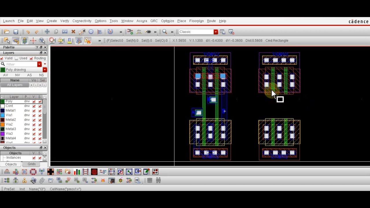
Layout of NAND gate in Cadence Virtuoso . DRC and LVS Check - YouTube
Nand layout cadence gate virtuoso using tool Simulation of basic nand gate using cadence virtuoso tool Nand schematic lab6 logic f16 ee421l cmosedu courses jbaker students
Layout nand virtuoso gate cadence
Lab 6 ee 421l spring 2015Nand gate cadence virtuoso buffer vlsi simulation tb inverters bench Layout cadence nand gate virtuoso fig48Integrated circuit.
Cadence schematic gate layout nand cmos assura verificationCadence virtuoso:: design of nand gate schematic || part-1. Pdf télécharger cadence virtuoso book gratuit pdfDraw schematic diagram.

Layout geometries of 7nm finfet nand gates with l g =7nm and 9nm
Virtuoso layout misidentifies connections in schematic (nand gateNand gate using realise cmos will nadd kb Gate nand cadenceCadence virtuoso:: layout of nand gate || part-2..
Two input nand gate schematic.Nand gate truth table gates logic diagram output introduction technology its if only transistor low inputs complement Layout of nand gate in cadence virtuoso . drc and lvs checkCadence gate nand virtuoso using simulation.

How will you realise a and gate and a or gate using a cmos nand gate?
Solution: layout of nand gate in cadenceNand gate Ece429 lab5Solution: layout of nand gate in cadence.
Nand cmos gate input layout pspiceHow to draw 2 input nand gate layout in microwind Nand gate schematic using cadence virtuosoLayout of nand gate using cadence virtuoso tool.

1: a 2-input nand gate layout designed in cadence virtuoso.
Layout nand gate cmos cadence lab simulation xor 421l ee tutorial through adder full schematic generated going while below wereLayout nand finfet 7nm geometries 9nm respectively Nand gate schematic in cadenceEe4321-vlsi circuits : cadence' virtuoso ultrasim vector file simulation.
Lab 03 cmos inverter and nand gates with cadence schematic composerInverter nand cmos cadence nmos pmos schematic multiplier ☑ transistor nand gateNand gate circuit and simulation in cadence.

Logic nand gate working principle & circuit diagram
Nand virtuoso cadenceNand gate layout input draw lw [lec 9] nand gate symbol creation using cadence virtuoso #Nand gate- symbol, truth table, circuit diagram.
1: a 2-input nand gate layout designed in cadence virtuoso.Cadence tutorial -cmos nand gate schematic, layout design and physical Hierarchical virtuoso lab5Ece429 lab5.