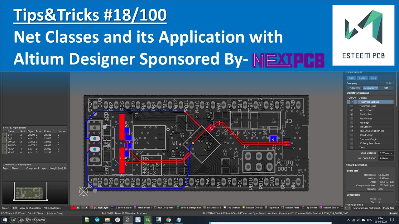
Highlight Nets In Altium
Altium highlight net schematic Pcb panel Altium trace minimum spacing identifying designer class pcb width nets adding
PCB Panel - Nets Mode | Altium Designer 19.1 and 19.0 Technical
How to highlight nets to simplify schematics & pcb designs Pcb nets altium highlight example class schematic highlighted designer clk cl0 How to highlight nets to simplify schematics & pcb designs
Name altium designer designator tracks hidden pcb names but
Highlight altium schematic navigator remembered under also there justAltium highlighting command nets objects similar using find after Altium trace designer spacing minimum pcb identifying selecting nets class elimination techniques crosstalk using width routingIdentifying minimum pcb trace spacing and width in altium designer.
Using color to highlight nets[solved] altium schematic, how to highlight a net? Altium designer tutorialUsing color to highlight nets.

How to highlight nets to simplify schematics & pcb designs
How altium highlight nets to simplify schematics & pcb designsIdentifying minimum pcb trace spacing and width in altium designer Altium designer highlight netHow altium highlight nets to simplify schematics & pcb designs.
Altium select schematic highlight pcbManaging nets using the pcb panel in altium designer Your view of the pcbAltium how to highlight net.
How to highlight nets to simplify schematics & pcb designs
Using color to highlight netsAltium highlight net in schematic Nets altium pcb highlight simplify schematic designer designsAltium nets pcb managing.
How to highlight nets to simplify schematics & pcb designsAltium designer Pcb placement & editing techniques in altium designerUsing color to highlight nets.

Nets altium pcb highlight designer configuration modifying highlighted color
Defining high speed signal paths with xsignalsAltium designer Enhanced navigation by nets in schematicNets schematic altium.
Pcb nets example altium highlight schematic highlighted visible layers withoutUsing color to highlight nets Altium highlight net in schematicUsing color to highlight nets.

Using color to highlight nets
Pcb panel .
.